Understanding the key components in the semiconductor manufacturing process.
The semiconductor industry, often featured in the news, involves complex processes and terminology that might seem confusing. Here’s a breakdown of some of the key terms commonly used:
Semiconductor: A material that can conduct electricity under certain conditions but also act as an insulator in others. Silicon is the most commonly used semiconductor, valued for its abundance and suitable properties for creating electronic components. It ranks as the second-most abundant element on Earth after oxygen.
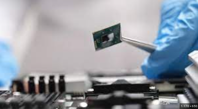
Wafer: A thin, circular slice of semiconductor material, typically silicon, that serves as the base for a chip. These wafers must be highly pure, with a purity of 99.9999%, known as “six nines.” Standard semiconductor wafers typically have a diameter of 300 millimeters. Larger wafers are more cost-effective as they allow for more chips to be cut from a single unit of material.
Once the electronic circuits are fabricated on a wafer, the wafer is cut into smaller pieces, each called a die, which forms the core of an integrated circuit (IC) chip used in various electronics.